This document describes an algorithmic method for generating modified nodal analysis (MNA) equations when the circuit has inductors, capacitors and/or operational amplifiers (op-amps). It consists of several parts:.
Applying modified nodal analysis to circuits with inductors and capacitors presents no special difficulty if one uses the complex impedance of these elements.
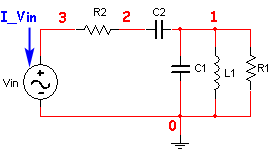
\[\eqalign{ {Z_R} &= R \hfill \\ {Z_{_L}} &= sL = j\omega L \hfill \\ {Z_C} &= \frac{1}{{sC}} = \frac{1}{{j\omega C}} \hfill \\ } \]Let us apply MNA to the following circuit (which already has nodes labeled, and the current through the voltage source defined and labeled):

MNA will generate 4 equations, one for each of the three nodes, and one for Vin. By inspection we get:
\[\eqalign{ v\_1 \cdot s \cdot C1 + \frac{{v\_1}}{{s \cdot L1}} + \frac{{v\_1}}{{R1}} + \left( {v\_1 - v\_2} \right) \cdot s \cdot C2 &= 0\quad \quad \quad &node\;1 \\ \frac{{v\_2 - v\_3}}{{R2}} + \left( {v\_2 - v\_1} \right) \cdot s \cdot C2 &= 0\quad \quad \quad &node\;2 \\ I\_Vin + \frac{{v\_3 - v\_2}}{{R2}} &= 0\quad \quad \quad &node\;3 \\ v\_3 &= Vin\quad \quad \quad &Vin \\ } \]Using the MNA algorithm we get:
\[\begin{gathered} {\mathbf{G}} = \left[ {\begin{array}{*{20}{c}} {s \cdot C1 + s \cdot C2 + \frac{1}{{s \cdot L1}} + \frac{1}{{R1}}}&{ - s \cdot C2}&0 \\ { - s \cdot C2}&{s \cdot C2 + \frac{1}{{R2}}}&{ - \frac{1}{{R2}}} \\ 0&{ - \frac{1}{{R2}}}&{\frac{1}{{R2}}} \end{array}} \right],\quad \quad {\mathbf{B}} = {{\mathbf{C}}^T} = \left[ {\begin{array}{*{20}{c}} 0 \\ 0 \\ 1 \end{array}} \right],\quad \quad {\mathbf{D}} = \left[ 0 \right] \\ {\mathbf{A}} = \left[ {\begin{array}{*{20}{c}} {s \cdot C1 + s \cdot C2 + \frac{1}{{s \cdot L1}} + \frac{1}{{R1}}}&{ - s \cdot C2}&0&0 \\ { - s \cdot C2}&{s \cdot C2 + \frac{1}{{R2}}}&{ - \frac{1}{{R2}}}&0 \\ 0&{ - \frac{1}{{R2}}}&{\frac{1}{{R2}}}&1 \\ 0&0&1&0 \end{array}} \right] \\ {\mathbf{v}} = \left[ {\begin{array}{*{20}{c}} {v\_1} \\ {v\_2} \\ {v\_3} \end{array}} \right],\quad \quad {\mathbf{j}} = \left[ {I\_Vin} \right],\quad \quad {\mathbf{x}} = \left[ {\begin{array}{*{20}{c}} {v\_1} \\ {v\_2} \\ {v\_3} \\ {I\_Vin} \end{array}} \right] \\ {\mathbf{i}} = \left[ {\begin{array}{*{20}{c}} 0 \\ 0 \\ 0 \end{array}} \right],\quad \quad {\mathbf{e}} = \left[ {Vin} \right],\quad \quad {\mathbf{z}} = \left[ {\begin{array}{*{20}{c}} 0 \\ 0 \\ 0 \\ {Vin} \end{array}} \right] \\ \end{gathered} \]
Since the matrices are all defined, we can now wirte the final matrices:
\[\begin{gathered} {\mathbf{Ax}} = {\mathbf{z}} \\ or \\ \left[ {\begin{array}{*{20}{c}} {s \cdot C1 + s \cdot C2 + \frac{1}{{s \cdot L1}} + \frac{1}{{R1}}}&{ - s \cdot C2}&0&0 \\ { - s \cdot C2}&{s \cdot C2 + \frac{1}{{R2}}}&{ - \frac{1}{{R2}}}&0 \\ 0&{ - \frac{1}{{R2}}}&{\frac{1}{{R2}}}&1 \\ 0&0&1&0 \end{array}} \right]\left[ {\begin{array}{*{20}{c}} {v\_1} \\ {v\_2} \\ {v\_3} \\ {I\_Vin} \end{array}} \right] = \left[ {\begin{array}{*{20}{c}} 0 \\ 0 \\ 0 \\ {Vin} \end{array}} \right] \\ \end{gathered} \]Careful inspection of this result verifies that it is identical to the original result. Don't worry about solving this equation; a later page will introduce SCAM - A MATLAB tool for deriving and solving circuit equations symbolically.
Applying modified nodal analysis to circuits with ideal operational amplifiers (op- amps) is a bit more difficult. Each op-amp increases the count of voltage sources by 1 (because the output of an op amp is treated as a voltage source), but also complicates the creation of the MNA matrices. In particular, the B and C matrices are no longer transposes of each other. To see how the ideal operational amplifier is handled, consider the circuit below:
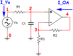
Note that we have labelled all of the nodes, and defined a current through each voltage source. The current through the voltage source Vs is I_Vs, and the voltage into the op-amp is labeled I_OA. We will make the standard assumption for an ideal op-amp. Namely that there is no current into the device at either input to the op-amp, and the voltage difference between the inputs is zero (note caveats below).
This circuit will require 6 equations -- one each for the 4 nodes and one each for the 2 labeled currents. We can now write the circuit equations by inspection.
\[\eqalign{ I\_Vs + \frac{{v\_1 - v\_2}}{{R1}} &= 0\quad \quad \;\quad &node\;1 \\ \frac{{v\_2 - v\_1}}{{R1}} + v\_2 \cdot s \cdot C1 &= 0\quad \quad \;\quad &node\;2 \\ \frac{{v\_3}}{{R3}} + \frac{{v\_3 - v\_4}}{{R2}} &= 0\quad \quad \;\quad &node\;3 \\ I\_OA + \frac{{v\_4 - v\_3}}{{R2}} &= 0\quad \quad \;\quad &node\;4 \\ v\_1 &= Vs\;\;\;\;\quad \;\,&Vs \\ v\_2 - v\_3 &= 0\quad \quad \quad \;&OpAmp\;inputs } \]or in matrix form:
\[\left[ {\begin{array}{*{20}{c}} {\frac{1}{{R1}}}&{ - \frac{1}{{R1}}}&0&0&1&0 \\ { - \frac{1}{{R1}}}&{\frac{1}{{R1}} + s \cdot C1}&0&0&0&0 \\ 0&0&{\frac{1}{{R2}} + \frac{1}{{R3}}}&{ - \frac{1}{{R2}}}&0&0 \\ 0&0&{ - \frac{1}{{R2}}}&{\frac{1}{{R2}}}&0&1 \\ 1&0&0&0&0&0 \\ 0&1&{ - 1}&0&0&0 \end{array}} \right]\left[ {\begin{array}{*{20}{c}} {v\_1} \\ {v\_2} \\ {v\_3} \\ {v\_4} \\ {I\_Vs} \\ {I\_OA} \end{array}} \right] = \left[ {\begin{array}{*{20}{c}} 0 \\ 0 \\ 0 \\ 0 \\ {Vs} \\ 0 \end{array}} \right]\]The only difference between this equation and the others that we have developed is that the equation for the op-amp is not in terms of the voltage at its output, but rather it specifies that the two input terminals are at the same potential.
The A matrix:
Recall that the A matrix is formed of four smaller matrices, G, B, C, and D.
The x matrix is unchanged.
The z matrix:
Recall that the z matrix is formed of two smaller matrices, i and e.
Caveats: The two ideal op-amp assumptions (no input current, no potential difference at inputs) only hold for circuits with negative feedback. Because of this, the MNA method as applied here can give erroneous results if negative feedback is not present. This problem actually persists in many commercial circuit simulators -- you can hook up a circuit with the input terminals reversed (so that it would not operate properly in practice due to lack of negative feedback) and the simulation behaves as if there is no problem. Note also that the output of the op-amp is not limited by any power supply -- this circuit will happily generate hundreds of volts.
Also: the op-amp rule can be simplified by taking advantage of the redundancy in node voltages since the two input nodes are at the same voltage. Taking advantage of this fact reduces the number of equations by 1, though it makes the generation of the equations a bit more difficult (The diagonal of the G matrix can have negative values, the off-diagonal element elements can be positive, the C matrix can have values besides 1, -1 and 0 and the D matrix is non-zero). See Litovski for details.
Let's apply the algorithm to the circuit at hand:

Using the rules for the algorithm we get:
\[\begin{gathered} {\mathbf{G}} = \left[ {\begin{array}{*{20}{c}} {\frac{1}{{R1}}}&{ - \frac{1}{{R1}}}&0&0 \\ { - \frac{1}{{R1}}}&{\frac{1}{{R1}} + s \cdot C1}&0&0 \\ 0&0&{\frac{1}{{R2}} + \frac{1}{{R3}}}&{ - \frac{1}{{R2}}} \\ 0&0&{ - \frac{1}{{R2}}}&{\frac{1}{{R2}}} \end{array}} \right],\; \\ {\mathbf{B}} = \left[ {\begin{array}{*{20}{c}} 1&0 \\ 0&0 \\ 0&0 \\ 0&1 \end{array}} \right],\;{\mathbf{C}} = \left[ {\begin{array}{*{20}{c}} 1&0&0&0 \\ 0&1&{ - 1}&0 \end{array}} \right],\;{\mathbf{D}} = \left[ {\begin{array}{*{20}{c}} 0&0 \\ 0&0 \end{array}} \right] \\ {\mathbf{A}} = \left[ {\begin{array}{*{20}{c}} {\frac{1}{{R1}}}&{ - \frac{1}{{R1}}}&0&0&1&0 \\ { - \frac{1}{{R1}}}&{\frac{1}{{R1}} + s \cdot C1}&0&0&0&0 \\ 0&0&{\frac{1}{{R2}} + \frac{1}{{R3}}}&{ - \frac{1}{{R2}}}&0&0 \\ 0&0&{ - \frac{1}{{R2}}}&{\frac{1}{{R2}}}&0&1 \\ 1&0&0&0&0&0 \\ 0&1&{ - 1}&0&0&0 \end{array}} \right] \\ {\mathbf{v}} = \left[ {\begin{array}{*{20}{c}} {v\_1} \\ {v\_2} \\ {v\_3} \\ {v\_4} \end{array}} \right],\;{\mathbf{j}} = \left[ {\begin{array}{*{20}{c}} {I\_Vs} \\ {I\_OA} \end{array}} \right],\quad {\mathbf{x}} = \left[ {\begin{array}{*{20}{c}} {\begin{array}{*{20}{c}} {v\_1} \\ {v\_2} \\ {v\_3} \\ {v\_4} \end{array}} \\ {\begin{array}{*{20}{c}} {I\_Vs} \\ {I\_OA} \end{array}} \end{array}} \right] \\ {\mathbf{i}} = \left[ {\begin{array}{*{20}{c}} 0 \\ 0 \\ 0 \\ 0 \end{array}} \right],\;{\mathbf{e}} = \left[ {\begin{array}{*{20}{c}} {Vs} \\ 0 \end{array}} \right],\quad {\mathbf{z}} = \left[ {\begin{array}{*{20}{c}} {\begin{array}{*{20}{c}} 0 \\ 0 \\ 0 \\ 0 \end{array}} \\ {\begin{array}{*{20}{c}} {Vs} \\ 0 \end{array}} \end{array}} \right] \\ \end{gathered} \]Putting evertything together yields:
\[\begin{gathered} {\mathbf{Ax}} = {\mathbf{z}} \\ or \\ \left[ {\begin{array}{*{20}{c}} {\frac{1}{{R1}}}&{ - \frac{1}{{R1}}}&0&0&1&0 \\ { - \frac{1}{{R1}}}&{\frac{1}{{R1}} + s \cdot C1}&0&0&0&0 \\ 0&0&{\frac{1}{{R2}} + \frac{1}{{R3}}}&{ - \frac{1}{{R2}}}&0&0 \\ 0&0&{ - \frac{1}{{R2}}}&{\frac{1}{{R2}}}&0&1 \\ 1&0&0&0&0&0 \\ 0&1&{ - 1}&0&0&0 \end{array}} \right]\left[ {\begin{array}{*{20}{c}} {\begin{array}{*{20}{c}} {v\_1} \\ {v\_2} \\ {v\_3} \\ {v\_4} \end{array}} \\ {\begin{array}{*{20}{c}} {I\_Vs} \\ {I\_OA} \end{array}} \end{array}} \right] = \left[ {\begin{array}{*{20}{c}} {\begin{array}{*{20}{c}} 0 \\ 0 \\ 0 \\ 0 \end{array}} \\ {\begin{array}{*{20}{c}} {Vs} \\ 0 \end{array}} \end{array}} \right] \\ \end{gathered} \]This result, upon inspection, is identical to our previous result.
Let's look at another simple example just to reinforce the concepts.
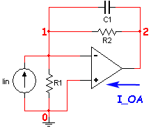
This circuit will require just 3 equations (2 nodes, 1 voltage sources). By inspection we get:
\[\eqalign{ - Iin + \frac{{v\_1}}{{R1}} + \left( {v\_1 - v\_2} \right) \cdot s \cdot C1 + \frac{{\left( {v\_1 - v\_2} \right)}}{{R2}} &= 0\quad \quad \;\quad &node\;1 \\ \left( {v\_2 - v\_1} \right) \cdot s \cdot C1 + \frac{{\left( {v\_2 - v\_1} \right)}}{{R2}} + I\_OA &= 0\quad \quad \;\quad &node\;2 \\ v\_2 - v\_1 &= 0 \\ 0 - v\_1 &= 0 \\ - v1 &= 0\quad \quad \;\quad &OpAmp\;inputs } \]Using our MNA algorithm we get:
\[\begin{gathered} {\mathbf{G}} = \left[ {\begin{array}{*{20}{c}} {\frac{1}{{R1}} + \frac{1}{{R2}} + s \cdot C1}&{ - \frac{1}{{R2}} - s \cdot C1} \\ { - \frac{1}{{R2}} - s \cdot C1}&{\frac{1}{{R2}} + s \cdot C1} \end{array}} \right],\;{\mathbf{B}} = \left[ {\begin{array}{*{20}{c}} 0 \\ 1 \end{array}} \right],\;{\mathbf{C}} = \left[ {\begin{array}{*{20}{c}} { - 1}&0 \end{array}} \right],\;{\mathbf{D}} = \left[ 0 \right] \\ {\mathbf{A}} = \left[ {\begin{array}{*{20}{c}} {\frac{1}{{R1}} + \frac{1}{{R2}} + s \cdot C1}&{ - \frac{1}{{R2}} - s \cdot C1}&0 \\ { - \frac{1}{{R2}} - s \cdot C1}&{\frac{1}{{R2}} + s \cdot C1}&1 \\ { - 1}&0&0 \end{array}} \right] \\ {\mathbf{v}} = \left[ {\begin{array}{*{20}{c}} {v\_1} \\ {v\_2} \end{array}} \right],\;{\mathbf{j}} = \left[ {I\_OA} \right],\quad {\mathbf{x}} = \left[ {\begin{array}{*{20}{c}} {\begin{array}{*{20}{c}} {v\_1} \\ {v\_2} \end{array}} \\ {I\_OA} \end{array}} \right] \\ {\mathbf{i}} = \left[ {\begin{array}{*{20}{c}} 1 \\ 0 \end{array}} \right],\;{\mathbf{e}} = \left[ 0 \right],\quad {\mathbf{z}} = \left[ {\begin{array}{*{20}{c}} {\begin{array}{*{20}{c}} Iin \\ 0 \end{array}} \\ 0 \end{array}} \right] \\ \end{gathered} \]We can now use these matrices to solve the circuit:
\[\begin{gathered} {\mathbf{Ax}} = {\mathbf{z}} \\ or \\ \left[ {\begin{array}{*{20}{c}} {\frac{1}{{R1}} + \frac{1}{{R2}} + s \cdot C1}&{ - \frac{1}{{R2}} - s \cdot C1}&0 \\ { - \frac{1}{{R2}} - s \cdot C1}&{\frac{1}{{R2}} + s \cdot C1}&1 \\ { - 1}&0&0 \end{array}} \right]\left[ {\begin{array}{*{20}{c}} {\begin{array}{*{20}{c}} {v\_1} \\ {v\_2} \end{array}} \\ {I\_OA} \end{array}} \right] = \left[ {\begin{array}{*{20}{c}} {\begin{array}{*{20}{c}} Iin \\ 0 \end{array}} \\ 0 \end{array}} \right] \\ \end{gathered} \]which agrees with our previous result.
The next document describes SCAM, a MATLAB program that performs all of these manipulations to set up the matrices, and then solves the circuit.