This document describes an algorithmic method for generating MNA (Modified Nodal Analysis) equations for systems with only resistors and idependent sources.. It consists of several parts:.
Many of the ideas and notation from this page are from Litovski, though the discussion here is quite simpler because only independent voltage and current sources are considered.
Recall from the previous document:
MNA applied to a circuit with only passive elements (resistors) and independent current and voltage sources results in a matrix equation of the form:
\[{\mathbf{Ax = z}}\]For a circuit with n nodes and m independent voltage sources:
The circuit is solved by a simple matrix manipulation:
\[{\mathbf{x = }}{{\mathbf{A}}^{ - 1}}{\mathbf{z}}\]Though this may be difficult by hand, it is straightforward and so is easily done by computer.
Obviously, the notation used does not change the solution. However the convention described below will make it quite easy to develop the matrices necessary for solution of the circuit.
These rules are somewhat restrictive (more so than they need to be) but they make development of the algorithm easier while still allowing quite a bit of freedom.
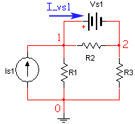
These rules are easily explained with an example (Example 3 from previous page):

This circuit is labeled according to the guidelines above. Ground is node 0 and the other two nodes are labeled 1 and 2. The voltage and current sources have labels with no underscores and the current through the voltage source Vs1 is labeled I_Vs1. We will discuss how to use this diagram (with these labels) to generate the MNA equations below.
There are three matrices we need to generate, the A matrix, the x matrix and the z matrix. Each of these will be created by combining several individual sub-matrices. To motivate the rules for generating the matrices we will consider the two sample circuits below (example 2 and example 3 from previous web page, with Notational Convention as above). I simply state the resulting MNA equations, but in the following text we will show how to generate each one.
| Case 1 |
| Circuit Diagram |
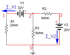 |
| Case 2 |
| Circuit Diagram |
 |
The A matrix will be developed as the combination of 4 smaller matrices, G, B, C, and D.
\[{\mathbf{A}} = \left[ {\begin{array}{*{20}{c}} {\mathbf{G}}&{\mathbf{B}} \\ {\mathbf{C}}&{\mathbf{D}} \end{array}} \right]\]The A matrix is (m+n)×(m+n) (n is the number of nodes, and m is the number of independent voltage sources) and:
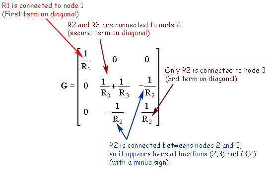
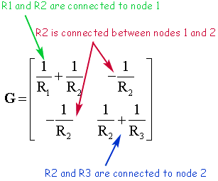
The G matrix is an n×n matrix formed in two steps
Demonstrations
| Case 1 | |
| Circuit Diagram | MNA Equations |
 |
\[{\mathbf{G}} = \left[ {\begin{array}{*{20}{c}} {\frac{1}{{{R_1}}}}&0&0 \\ 0&{\frac{1}{{{R_2}}} + \frac{1}{{{R_3}}}}&{ - \frac{1}{{{R_2}}}} \\ 0&{ - \frac{1}{{{R_2}}}}&{\frac{1}{{{R_2}}}} \end{array}} \right]\] |
 |
|
| Case 2 | |
| Circuit Diagram | MNA Equations |
 |
\[{\mathbf{G}} = \left[ {\begin{array}{*{20}{c}} {\frac{1}{{{R_1}}} + \frac{1}{{{R_2}}}}&{ - \frac{1}{{{R_2}}}} \\ { - \frac{1}{{{R_2}}}}&{\frac{1}{{{R_2}}} + \frac{1}{{{R_3}}}} \end{array}} \right]\] |
 |
|
If an element is grounded, it will only have contribute to one entry in the G matrix -- at the appropriate location on the diagonal. If it is ungrounded it will contribute to four entries in the matrix -- two diagonal entries (corresponding to the two nodes) and two off-diagonal entries.
The B matrix is an n×m matrix with only 0, 1 and -1 elements. Each location in the matrix corresponds to a particular voltage source (first dimension) or a node (second dimension). If the positive terminal of the ith voltage source is connected to node k, then the element (i,k) in the B matrix is a 1. If the negative terminal of the ith voltage source is connected to node k, then the element (i,k) in the B matrix is a -1. Otherwise, elements of the B matrix are zero.
Demonstrations
| Case 1 | |
| Circuit Diagram | MNA Equations |
 |
\[{\mathbf{B}} = \left[ {\begin{array}{*{20}{c}} { - 1}&0 \\ 1&0 \\ 0&1 \end{array}} \right]\] |
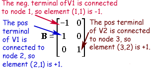 |
|
| Case 2 | |
| Circuit Diagram | MNA Equations |
 |
\[{\mathbf{B}} = \left[ {\begin{array}{*{20}{c}} 1 \\ { - 1} \end{array}} \right]\] |
If a voltage source is ungrounded, it will have two elements in the B matrix (a 1 and a -1 in the same column). If it is grounded it will only have one element in the matrix.
The C matrix is an m×n matrix with only 0, 1 and -1 elements. Each location in the matrix corresponds to a particular node (first dimension) or voltage source (second dimension). If the positive terminal of the ith voltage source is connected to node k, then the element (k,i) in the C matrix is a 1. If the negative terminal of the ith voltage source is connected to node k, then the element (k,i) in the C matrix is a -1. Otherwise, elements of the C matrix are zero.
In other words, the C matrix is the transpose of the B matrix. (This is not the case when dependent sources are present.)
Case 1: ${\mathbf{C}} = \left[ {\begin{array}{*{20}{c}} { - 1}&1&0 \\ 0&0&1 \end{array}} \right]$
Case 2: ${\mathbf{C}} = \left[ {\begin{array}{*{20}{c}} 1&{ - 1} \end{array}} \right]$
The D matrix is an m×m matrix that is composed entirely of zeros. (It can be non-zero if dependent sources are considered.)
Case 1: ${\mathbf{D}} = \left[ {\begin{array}{*{20}{c}} 0&0 \\ 0&0 \end{array}} \right]$
Case 2: ${\mathbf{D}} = \left[ 0 \right]$
The x matrix holds our unknown quantities and will be developed as the combination of 2 smaller matrices v and j. It is considerably easier to define than the A matrix.
\[{\mathbf{x}} = \left[ {\begin{array}{*{20}{c}} {\mathbf{v}} \\ {\mathbf{j}} \end{array}} \right]\]The x matrix is (m+n)×1 (n is the number of nodes, and m is the number of independent voltage sources) and:
The v matrix is an n×1 matrix formed of the node voltages. Each element in v corresponds to the voltage at the equivalent node in the circuit (there is no entry for ground -- node 0).
For example if a circuit has three nodes, the v matrix is
\[{\mathbf{v}} = \left[ {\begin{array}{*{20}{c}} {v\_1} \\ {v\_2} \\ {v\_3} \end{array}} \right]\]For a circuit with n nodes we get
\[{\mathbf{v}} = = \left[ {\begin{array}{*{20}{c}} {v\_1} \\ \vdots \\ {v\_n} \end{array}} \right]\]and so on.
The j matrix is an m×1 matrix, with one entry for the current through each voltage source. So if there are two voltage sources V1 and V2, the j matrix will be:
\[{\mathbf{j}} = \left[ {\begin{array}{*{20}{c}} {i\_V1} \\ {i\_V2} \end{array}} \right]\]Demonstrations for the x matrix.
| Case 1 | |
| Circuit Diagram | MNA Equations |
 |
\[{\mathbf{v}} = \left[ {\begin{array}{*{20}{c}} {v\_1} \\ {v\_2} \\ {v\_3} \end{array}} \right],\;{\mathbf{j}} = \left[ {\begin{array}{*{20}{c}} {i\_V1} \\ {i\_V2} \end{array}} \right],\quad {\mathbf{x}} = \left[ {\begin{array}{*{20}{c}} {\mathbf{v}} \\ {\mathbf{j}} \end{array}} \right] = \left[ {\begin{array}{*{20}{c}} {\begin{array}{*{20}{c}} {v\_1} \\ {v\_2} \\ {v\_3} \end{array}} \\ {\begin{array}{*{20}{c}} {i\_V1} \\ {i\_V2} \end{array}} \end{array}} \right]\] |
| Case 2 | |
| Circuit Diagram | MNA Equations |
 |
\[{\mathbf{v}} = \left[ {\begin{array}{*{20}{c}} {v\_1} \\ {v\_2} \end{array}} \right],\;{\mathbf{j}} = \left[ {i\_Vs1} \right],\quad {\mathbf{x}} = \left[ {\begin{array}{*{20}{c}} {\mathbf{v}} \\ {\mathbf{j}} \end{array}} \right] = \left[ {\begin{array}{*{20}{c}} {\begin{array}{*{20}{c}} {v\_1} \\ {v\_2} \end{array}} \\ {i\_Vs1} \end{array}} \right]\] |
The z matrix holds our independent voltage and current sources and will be developed as the combination of 2 smaller matrices i and e. It is quite easy to formulate.
\[{\mathbf{z = }}\left[ {\begin{array}{*{20}{c}} {\mathbf{i}} \\ {\mathbf{e}} \end{array}} \right]\]The z matrix is (m+n)×1 (n is the number of nodes, and m is the number of independent voltage sources) and:
The i matrix is an n×1 matrix with each element of the matrix corresponding to a particular node. The value of each element of i is determined by the sum of current sources into the corresponding node. If there are no current sources connected to the node, the value is zero.
The e matrix is an m×1 matrix with each element of the matrix equal in value to the corresponding independent voltage source.
Demonstrations for the z matrix.
| Case 1 | |
| Circuit Diagram | MNA Equations |
 |
\[{\mathbf{i}} = \left[ {\begin{array}{*{20}{c}} 0 \\ 0 \\ 0 \end{array}} \right],\;{\mathbf{e}} = \left[ {\begin{array}{*{20}{c}} {V1} \\ {V2} \end{array}} \right],\quad {\mathbf{z}} = \left[ {\begin{array}{*{20}{c}} {\begin{array}{*{20}{c}} 0 \\ 0 \\ 0 \end{array}} \\ {\begin{array}{*{20}{c}} {V1} \\ {V2} \end{array}} \end{array}} \right]\] |
| Case 2 | |
| Circuit Diagram | MNA Equations |
 |
\[{\mathbf{i}} = \left[ {\begin{array}{*{20}{c}} {Is1} \\ 0 \end{array}} \right],\;{\mathbf{e}} = \left[ {Vs1} \right],\quad {\mathbf{z}} = \left[ {\begin{array}{*{20}{c}} {\begin{array}{*{20}{c}} {Is1} \\ 0 \end{array}} \\ {Vs1} \end{array}} \right]\] |
We can now write out the full matrix solutions for both cases that we have been developing.
| Case 1 | |
| Circuit Diagram | MNA Equations |
 |
\[\left[ {\begin{array}{*{20}{c}} {\frac{1}{{{R_1}}}}&0&0&{ - 1}&0 \\ 0&{\frac{1}{{{R_2}}} + \frac{1}{{{R_3}}}}&{ - \frac{1}{{{R_2}}}}&1&0 \\ 0&{ - \frac{1}{{{R_2}}}}&{\frac{1}{{{R_2}}}}&0&1 \\ { - 1}&1&0&0&0 \\ 0&0&1&0&0 \end{array}} \right]\left[ {\begin{array}{*{20}{c}} {\begin{array}{*{20}{c}} {v\_1} \\ {v\_2} \\ {v\_3} \end{array}} \\ {\begin{array}{*{20}{c}} {i\_V1} \\ {i\_V2} \end{array}} \end{array}} \right] = \left[ {\begin{array}{*{20}{c}} {\begin{array}{*{20}{c}} 0 \\ 0 \\ 0 \end{array}} \\ {\begin{array}{*{20}{c}} {V1} \\ {V2} \end{array}} \end{array}} \right]\] |
| Case 2 | |
| Circuit Diagram | MNA Equations |
 |
\[\left[ {\begin{array}{*{20}{c}} {\frac{1}{{{R_1}}} + \frac{1}{{{R_2}}}}&{ - \frac{1}{{{R_2}}}}&1 \\ { - \frac{1}{{{R_2}}}}&{\frac{1}{{{R_2}}} + \frac{1}{{{R_3}}}}&{ - 1} \\ 1&{ - 1}&0 \end{array}} \right]\left[ {\begin{array}{*{20}{c}} {\begin{array}{*{20}{c}} {v\_1} \\ {v\_2} \end{array}} \\ {i\_Vs1} \end{array}} \right] = \left[ {\begin{array}{*{20}{c}} {\begin{array}{*{20}{c}} {Is1} \\ 0 \end{array}} \\ {Vs1} \end{array}} \right]\] |
So far we have only dealt with resistors and independent voltage and current sources. The next document will show that adding capacitors and inductors is trivial, and adding op-amps only adds minimally to the difficulty.